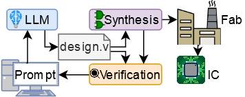
TL;DR: I architectured a microcontroller chip in early 2023 using ChatGPT and it was taped out. Now it controls my christmas tree.
This was the first time anyone had used an LLM to design silicon. Our paper appeared at MLCAD’23, arXiv link.
All chat logs are provided in our repository and QTcore-C1 GitHub.
The full story: Part 1, the Idea
In March of this year a post made it to the front page of Hacker News regarding Tiny Tapeout. Here, they had made a process where you could submit custom, miniature silicon designs to a subset of a silicon shuttle for just $100.
At the time, I was working at NYU on my postdoc, which among other things, was exploring the use of Large Language Models for Verilog. We were benchmarking a variety of different applications for the use of LLMs like ChatGPT for designing hardware, including in specification interpretation, design, and bug detection and repair. We were one of the very first movers in this space, using GPT-2 and Verilog all the way back in 2020.
I was immediately interested, then, in the HN post. We’d always been working with FPGAs and simulations due to the prohibitive cost of a real tapeout. But, there’s always a simulation-reality gap, so showing that LLMs and AI really could produce chips could be a boon for our research area. Could we use Tiny Tapeout as a vehicle for this - and use an LLM to not just write Verilog, but also to design the Verilog for a real chip?
I spoke to my supervisors, and several other Ph.D students, and we brainstormed a few ideas. Tiny Tapeout is extremely small - just a thousand standard cells or so, meaning that the design would be very constrained, but we all really liked the idea, especially as it seemed nobody had done it yet - so if we moved quickly, we might be able to do a world’s-first!
So, we decided to go for it. But now, there were many other things to consider. What should we submit, given the design space was so small? And there are other concerns too. We knew from our own prior work that LLMs can write hardware design languages like Verilog, but they just aren’t very good at it, with much higher incidences of syntax or logic errors compared with more popular languages like Python - This is actually why me and my team have produced our own LLMs for Verilog, but I digress. So we needed to decide - if we did want to make a chip using an LLM, (1) which LLM should we use? (2) How much help should we give it? (3) What prompting strategy should we try?
Part 2: Designing a methodology
We first decided on the LLMs. Instead of using the ‘autocomplete’ style LLMs which we had been working with up to this point, primarily OpenAI’s Codex and Salesforce CodeGen, we’d use the newer and flashier ‘conversational’ / ‘instructional’ style LLMs. We picked OpenAI’s ChatGPT, versions 3.5 and 4, Google’s Bard, and the open-source HuggingChat.
We then worked out two methods. The first would try and have the LLMs complete everything in a kind of feedback loop, whereby the LLM would be given a specification, then produce both the design and the tests for that design. A human would then run the tests and design in a simulator (iVerilog) and then return any errors to the LLM.
However, we knew from experience that LLMs are also fairly silly sometimes, and can get stuck in loops where they think they are fixing a problem or improving an output when really they’re just iterating over the same data. So we theorized that we might need to give back ‘human assistance’ sometimes.
Through some preliminary experimentation, we decided on an initial process that looked like this:
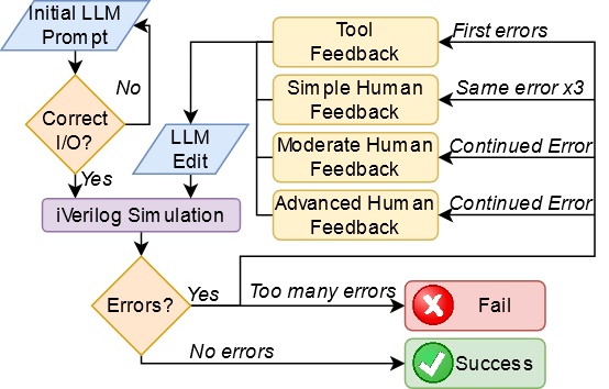
Ideally, the human would not need to provide much input, but this remained to be seen…
On the hardware tapeout side, we were targeting Tiny Tapeout 3, which would be based on a Skywater 130nm shuttle. It had constraints: the aforementioned 1000 standard cells, as well as only 8 bits of input (inclusive of any clock or reset) and 8 bits of output. Tiny Tapeout uses OpenLane, meaning we are also restricted to synthesizable Verilog-2001.
Part 3: What to design?
In the early stages of this experiment, we were interested in the potential for a standardized and (ideally) automatable flow for interacting with the conversational LLMs which would start from a specification and result in the hardware description language for that design. Given that we have 8 bits of input, we decided we could use 3 of these bits to control a design select mux to then fit in 8 small benchmarks. If these went well, we’d then work on something more ambitious.
These were the benchmarks that we came up with:
| Benchmark | Description |
|---|---|
| 8-bit Shift Register | Shift register with enable |
| Sequence Generator | Generates a specific sequence of eight 8-bit values |
| Sequence Detector | Detects if the correct 8 3-bit inputs were given consecutively |
| ABRO FSM | One-hot state machine for detecting inputs A and B to emit O |
| Binary to BCD | Converts a 5-bit binary input into an 8-bit BCD output |
| LFSR | 8-bit Linear Feedback Shift Register |
| Traffic Light FSM | Cycle between 3 states based on a number of clock cycles |
| Dice Roller | Simulated rolling either a 4, 6, 8, or 20-sided die |
Each benchmark had a short specification describing it and its I/O, as well as the correct intended behaviour.
An NYU Ph.D. student, Jason Blocklove, then sat with the four chosen LLMs (ChatGPT-3.5, ChatGPT-4, Bard, and HuggingChat) and performed the process described earlier, shepherding the LLM through generating first the designs and then the testbenches, before simulating them together, and feeding back any errors.
Sometimes, special circumstances needed to be taken into account within the conversations. Due to the limits placed on how much output a model could give in a single response, files or explanations would often be cut off from finishing; in those cases the model would be prompted with ``Please continue’’. The code following a continue often started from before the final line of the earlier message, so when the code was copied into the file for compilation and simulation it was edited to form a cohesive block. However, no additional HDL was added for this process. Similarly, there were occasions when responses included comments for the user to add their own code. If these comments would prevent functionality, such as leaving an incomplete array of values, the response would be regenerated, otherwise it was left as-is.
Design prompts:
A design prompt here looked something like this:
I am trying to create a Verilog model for a shift register. It must meet the following specifications:

- Inputs:
	- Clock
	- Active-low reset
	- Data (1 bit)
	- Shift enable
- Outputs:
	- Data (8 bits)

How would I write a design that meets these specifications?
The returned designs varied in quality, and we found that only ChatGPT-4 could produce designs reliably. Here’s an example from each LLM for the first design, a shift register:
(These are clickable links, click to expand them)
ChatGPT-4
module shift_register (
    input wire clk,
    input wire reset_n,
    input wire data_in,
    input wire shift_enable,
    output reg [7:0] data_out
);

always @(posedge clk or negedge reset_n) begin
    if (!reset_n) begin
        data_out <= 8'b0; // Active-low reset: Clear the register when reset_n is low
    end else if (shift_enable) begin
        data_out <= {data_out[6:0], data_in}; // Shift the register and insert the new data bit
    end
end

endmodule
It works!
ChatGPT-3.5
module shift_register(
    input clk,
    input reset_n,
    input data,
    input shift_enable,
    output reg [7:0] q
);

always @(posedge clk, negedge reset_n) begin
    if (!reset_n) begin
        q <= 8'b0;
    end else if (shift_enable) begin
        q <= {q[6:0], data};
    end
end

endmodule
It works!
Bard
module shift_register (
  input clk,
  input rst,
  input [7:0] data,
  input shift_enable,
  output reg [7:0] data_out
);

  always @(posedge clk or posedge rst) begin
    if (rst) begin
      data_out <= 8'b0;
    end else begin
      if (shift_enable) begin
        data_out <= {data_out[6:0], data};
      end
    end
  end
It does not work! Notice the error in the definition of the data input!
HuggingChat
module ShiftRegister(input clk, input rst_n, input data_in, input shft_en, output reg [7:0] q);

// clock cycle of 22 ns
parameter CLK_CYCLE = 50;
parameter ADDR = 32'h0000641A; // default address for the CY7B974 EEPROM/flash control unit
parameter DATAW = 32'b1111000010000001000000000000000; // set default value of all registers from datasheet page B-21
parameter SP = 32'h015F;
parameter PE = 16'd1; // always for Vdd level detection. Set according to section "VIO Power Supply Voltage Monitoring" in datasheet p.13
parameter UDEN = 32'hFFFE; // unused device disable register
parameter VIDEN = 32'hFCED; // VIN/AN pin access disabled
parameter ADCDPF = 32'hFF7A; // alternative digital power supply voltage monitor config (ADP_SAR)
parameter _90FSYSCLKS = "Disabled"; // unused 1 byte register at offset 0x90 from FSMC_NORSRAM Timing Control Register. Read as zero if not used
parameter TRASETNEGL = 32'hFFFFFFFFFFFF;

assign data_out = ~data_in & shft_en & rst_n ? 1'b0 : (q[7:1] << 1) | {1'b0, data_in};
always @(*) begin
    # /* x'FF  */ CLK_RQSTDCLK *;

    # /reset_n R0 R0[(int*)&(_CTL--)] <= 32'h8000_0000;
    if (rst_n && !shft_en) begin
        $setuphold (posedge reset_n , negedge active ) ;
        $display("*** RESET ***\n");
        `#addr `addr:`addr[(int*) &POS]`pos ?(int) ( ((`addr`:addr[_ADDR]+ $_INTRTVALU)/2):1'b1;`addr:(addr<>`addr)`pos ,"Full scan done."));`cout!="Division by zero!" & '@( !_LUT) && (`grandpa')?(sprintf(`snip`,strlen(&_TI),($half*`cout>&1)'hash ()): snprintf(!reserve2((const char*)(type(*``cout)strlen`buf++->_GBIT])))) oe=tmp2 && tmp3 ? (__flash)((void*)realloc($(int*)(idx=(*(u*`ptr`)|(~(address><:sizeof(mtemp))))))) : (tmp1 || net$c) $(tie || leak$_parsefree()`load($_VO))`store(:)*value#stdh::)(`scan`:uint8_t RF)(addr<=&)> //Multiple errors\n');}  }}} end else if (!active_high && active)^begin €high end}begin€ pos bpoz,eu Europozize w; Pos file NewHdrPos Wrf `ezed=` Pos MaxRow=?[issued&tested]`specif bypa=end><changed *alpha sys varsub EOF varbb atEnd of call seq`,} else if (!endswith "\\") or myword`title==addr){droplocalvar hNextCutJob) ~sym\_name eof .~stop$; genw syncestrings TryEnd [] sizewriter(1)} if !=size( (`dynSym-NM compilersUDOVARSYMBOL))*~(uint2base NUMSERVER+" compiled")){clip0 clrw $addelem}\n\resources} subbytes wrdfmt removecomments Tr1ESran diff gred$\elleoformatfloat format----------------------`charTmpLim} Len rollover Leng len Len Non Rollovr OptimizationCenter}\n resident AsymptoticAspect}\np ResetOpt \All %par ID == PCI0 SPC ReconfigurationFeature supported } IF PROPRIETARY ASPECT=`port!\Plug
Oh dear… It appears to have gone insane :(
Testbenches
Once we had a design, we had to prompt for a testbench:
Can you create a Verilog testbench for this design? It should be self-checking and made to work with iverilog for simulation and validation. If test cases should fail, the testbench should provide enough information that the error can be found and resolved.
An example conversation
Here’s the complete flow of a conversation using ChatGPT-4.
Click to expand
USER:I am trying to create a Verilog model for a shift register. It must meet the following specifications:
- Inputs:
	- Clock
	- Active-low reset
	- Data (1 bit)
	- Shift enable
- Outputs:
	- Data (8 bits)
How would I write a design that meets these specifications?
ASSISTANT:
To create a Verilog model for an 8-bit shift register meeting the given specifications, you can follow this example:
module shift_register (
    input wire clk,
    input wire reset_n,
    input wire data_in,
    input wire shift_enable,
    output reg [7:0] data_out
);

always @(posedge clk or negedge reset_n) begin
    if (!reset_n) begin
        data_out <= 8'b0; // Active-low reset: Clear the register when reset_n is low
    end else if (shift_enable) begin
        data_out <= {data_out[6:0], data_in}; // Shift the register and insert the new data bit
    end
end

endmodule1. Define the `shift_register` module with the specified inputs and outputs.
2. Create an always block that responds to the rising edge of the clock (`posedge clk`) or the falling edge of the active-low reset (`negedge reset_n`).
3. Within the always block, check if the reset signal is low (`!reset_n`). If so, clear the 8-bit output register (`data_out <= 8'b0`).
4. If the reset signal is not low, check if the shift enable signal is high. If so, shift the data in the output register to the left and insert the new data bit at the least significant bit position (`data_out <= {data_out[6:0], data_in}`).
This design meets the given specifications and provides an 8-bit shift register with the desired inputs and outputs.
USER:
Can you create a Verilog testbench for this design? It should be self-checking and made to work with iverilog for simulation and validation. If test cases should fail, the testbench should provide enough information that the error can be found and resolved.
ASSISTANT:
Certainly! Here's a self-checking testbench for the 8-bit shift register design using iverilog:
`timescale 1ns/1ps

module tb_shift_register;
    reg clk;
    reg reset_n;
    reg data_in;
    reg shift_enable;
    wire [7:0] data_out;

    // Instantiate the shift_register module
    shift_register uut (
        .clk(clk),
        .reset_n(reset_n),
        .data_in(data_in),
        .shift_enable(shift_enable),
        .data_out(data_out)
    );

    // Clock generation
    always begin
        #5 clk = ~clk;
    end

    // Testbench stimulus
    initial begin
        // Initialize signals
        clk = 0;
        reset_n = 0;
        data_in = 0;
        shift_enable = 0;

        // Apply reset
        #10 reset_n = 1;
        #10 reset_n = 0;
        #10 reset_n = 1;

        // Test case 1: Simple shift
        data_in = 1'b1;
        shift_enable = 1'b1;
        repeat (8) @(posedge clk);
        if (data_out !== 8'b10000000) $display("Error: Test case 1 failed. Expected: 10000000, Received: %b", data_out);

        // Test case 2: Shift with alternating bits
        data_in = 1'b0;
        @(posedge clk);
        data_in = 1'b1;
        @(posedge clk);
        data_in = 1'b0;
        @(posedge clk);
        data_in = 1'b1;
        @(posedge clk);
        data_in = 1'b0;
        @(posedge clk);
        data_in = 1'b1;
        @(posedge clk);
        data_in = 1'b0;
        @(posedge clk);
        data_in = 1'b1;
        @(posedge clk);
        if (data_out !== 8'b10101010) $display("Error: Test case 2 failed. Expected: 10101010, Received: %b", data_out);

        // Test case 3: Shift without shift_enable
        data_in = 1'b0;
        shift_enable = 1'b0;
        @(posedge clk);
        if (data_out !== 8'b10101010) $display("Error: Test case 3 failed. Expected: 10101010, Received: %b", data_out);

        // Test case 4: Reset during shift operation
        data_in = 1'b1;
        shift_enable = 1'b1;
        @(posedge clk);
        reset_n = 0;
        @(posedge clk);
        reset_n = 1;
        if (data_out !== 8'b00000000) $display("Error: Test case 4 failed. Expected: 00000000, Received: %b", data_out);

        // Display success message and end simulation
        $display("All test cases passed!");
        $finish;
    end

endmodule1. Simple shift: Shifts 1 into the register and checks the output.
2. Shift with alternating bits: Shifts a pattern of alternating bits and checks the output.
3. Shift without shift_enable: Verifies that the shift register does not shift without the shift_enable signal.
4. Reset during shift operation: Checks if the register resets correctly during a shift operation.
The testbench provides error messages if any of the test cases fail. If all test cases pass
USER:
When running the simulation it gives the following output. Please provide fixed code.
Error: Test case 1 failed. Expected: 10000000, Received: 01111111
Error: Test case 2 failed. Expected: 10101010, Received: 01010101
Error: Test case 3 failed. Expected: 10101010, Received: 01010101
All test cases passed!
ASSISTANT:
Apologies for the confusion. It appears that the test cases are failing due to incorrect output expectations. I made a mistake in the test case expectations. Let's correct the test cases and update the testbench code:
`timescale 1ns/1ps

module tb_shift_register;
    reg clk;
    reg reset_n;
    reg data_in;
    reg shift_enable;
    wire [7:0] data_out;

    // Instantiate the shift_register module
    shift_register uut (
        .clk(clk),
        .reset_n(reset_n),
        .data_in(data_in),
        .shift_enable(shift_enable),
        .data_out(data_out)
    );

    // Clock generation
    always begin
        #5 clk = ~clk;
    end

    // Testbench stimulus
    initial begin
        // Initialize signals
        clk = 0;
        reset_n = 0;
        data_in = 0;
        shift_enable = 0;

        // Apply reset
        #10 reset_n = 1;
        #10 reset_n = 0;
        #10 reset_n = 1;

        // Test case 1: Simple shift
        data_in = 1'b1;
        shift_enable = 1'b1;
        repeat (8) @(posedge clk);
        if (data_out !== 8'b01111111) $display("Error: Test case 1 failed. Expected: 01111111, Received: %b", data_out);

        // Test case 2: Shift with alternating bits
        data_in = 1'b0;
        @(posedge clk);
        data_in = 1'b1;
        @(posedge clk);
        data_in = 1'b0;
        @(posedge clk);
        data_in = 1'b1;
        @(posedge clk);
        data_in = 1'b0;
        @(posedge clk);
        data_in = 1'b1;
        @(posedge clk);
        data_in = 1'b0;
        @(posedge clk);
        data_in = 1'b1;
        @(posedge clk);
        if (data_out !== 8'b01010101) $display("Error: Test case 2 failed. Expected: 01010101, Received: %b", data_out);

        // Test case 3: Shift without shift_enable
        data_in = 1'b0;
        shift_enable = 1'b0;
        @(posedge clk);
        if (data_out !== 8'b01010101) $display("Error: Test case 3 failed. Expected: 01010101, Received: %b", data_out);

        // Test case 4: Reset during shift operation
        data_in = 1'b1;
        shift_enable = 1'b1;
        @(posedge clk);
        reset_n = 0;
        @(posedge clk);
        reset_n = 1;
        if (data_out !== 8'b00000000) $display("Error: Test case 4 failed. Expected: 00000000, Received: %b", data_out);

        // Display success message and end simulation
        $display("All test cases passed!");
        $finish;
    end

endmodule(And it did pass without errors!)
Basic results
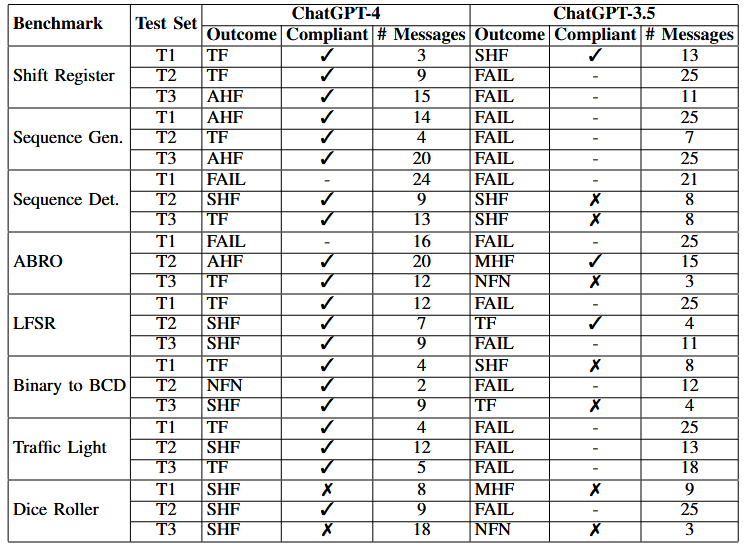
Overall, only ChatGPT-3.5 and -4 could produce designs reliably, so we only ended up analyzing these two models and excluded Bard and HuggingChat from our results. Using the two OpenAI models we finished off the full suite of benchmarks 3 times, and got the following results:
Nomenclature:
If no errors are reported then the design passes with no feedback necessary (NFN). If instead either of those actions report errors they are fed back into the model and it is asked to ``Please provide fixes.’’, referred to as tool feedback (TF). If the same error or type of error appears three times then simple human feedback (SHF) is given by the user, usually by stating what type of problem in Verilog would cause this error (e.g. syntax error in declaring a signal). If the error continues, moderate human feedback (MHF) is given with slightly more directed information being given to the tool to identify the specific error, and if the error persists then advanced human feedback (AHF) is given which relies on pointing out precisely where the error is and the method of fixing it. Once the design compiles and simulates with no failing test cases, it is considered a success. If however advanced feedback does not fix the error or should the user need to write any Verilog to address the error, the test is considered a failure. The test is also considered a failure if the conversation exceeds 25 messages, matching the OpenAI rate limit on ChatGPT-4 messages per 3 hours.
You can actually see all the chat logs in our repository (scripted benchmarks folder).
ChatGPT-4 performed well. The majority of benchmarks passed, most of which only required tool feedback. ChatGPT-4 most frequently needed human feedback in testbench design.
Several failure modes were consistent, with a common error being the addition of SystemVerilog-specific syntax in the design or testbench. For example, it would often try to use typedef to create states for the FSM models, or instantiate arrays of vectors, neither of which are supported in Verilog-2001.
In general, the testbenches produced by ChatGPT-4 were not particularly comprehensive. Still, the majority of the designs that passed their accompanying testbenches were also deemed to be compliant. The two non-compliant `passes’ were Dice Rollers which did not produce a pseudo-random output. The Dice Roller from test set T1 would output a 2 for one roll and then only 1 for all subsequent rolls, regardless of the die selected. Meanwhile, Dice Roller T3 would change values, but only between a small set (dependent on the chosen die) which rapidly repeated. To close the design loop, we synthesized test set T1 from the ChatGPT-4 conversations for Tiny Tapeout 3, adding in a wrapper module that was designed, but not tested, by ChatGPT-4. In all the design took 85 combinational logic units, 4 diodes, 44 flip flops, 39 buffers, and 300 taps to implement.
ChatGPT-3.5 performed notably worse than ChatGPT-4, with the majority of the conversations resulting in a failed benchmark, and the majority of those that passed their own testbenches being non-compliant. The modes of failure were less consistent with ChatGPT-3.5 than they were for ChatGPT-4, with a wide variety of issues introduced between each conversation and benchmark. It required corrections to the design and the testbenches far more often than ChatGPT-4.
Observations
Only ChatGPT-4 performed adequately for the purposes of writing Verilog, though it still required human feedback for most conversations to be both successful and compliant with the given specifications. When fixing errors, ChatGPT-4 would often require several messages to fix minor errors, as it struggled to understand exactly what specific Verilog lines would cause the error messages from iverilog. The errors it would add also tended to repeat themselves between conversations quite often.
ChatGPT-4 also struggled much more to create functioning testbenches than functioning designs. The majority of benchmarks required little to no modification of the design itself, instead necessitating testbench repair. This is particularly true of FSMs, as the model seemed unable to create a testbench which would properly check the output without significant feedback regarding the state transitions and corresponding expected outputs. ChatGPT-3.5, on the other hand, struggled with both testbenches and functional designs.
Part 4: Something more complex: The QTcore-A1
Having observed and helped the Ph.D. student with ChatGPT-4 during the benchmarks, I was now ready to take on a larger challenge, and set out to get it to create the components for a microcontroller. I wanted to know if unstructured conversations could lead to greater levels of performance from the model, using a kind of mutual creativity to write the design faster.
I will note here that I am an experienced engineer in the design of small, toy/academic processors, having taught students in this area for multiple years at the University of Auckland, New York University, and now at my current institution the University of New South Wales in Sydney Australia.
This was what I wanted ChatGPT-4 to build here. Knowing that we were working with extreme space limitations, I decided on an 8-bit accumulator-based architecture. Using a Von Neumann design (shared program and data memory) would save additional space, and then restricing that shared memory to just 32 bytes was my guess at something that would fit.
I decided that ChatGPT-4 would write every line of functional Verilog, but given the difficulties we had faced with verification and testbenches I would produce those and run and interpret the simulations etc.
Why make this design instead of something like RISC-V?: There are many implementations of open-source processors for ISAs like RISC-V and MIPS. The problem is, that means GPT-4 has seen these designs during training. For this work, I didn’t want to explore simply the capabilities of ChatGPT-4 to emit data it has trained over - rather, I wanted to see how it performed when making something more novel. As such, I shephereded the models into making a wholly new design, with a strange ISA that ChatGPT-4 itself provided, something I believe is quite different to what is available in the open-source literature.
I began with:
Let us make a brand new microprocessor design together. We're severely constrained on space and I/O. We have to fit in 1000 standard cells of an ASIC, so I think we will need to restrict ourselves to an accumulator based 8-bit architecture with no multi-byte instructions. Given this, how do you think we should begin?
The microprocessor design process began by defining the Instruction Set Architecture (ISA), then implementing components that the ISA would require, before combining those components in a datapath with a control unit to manage them. Simulation and testing were used to find bugs which were then repaired.
Structuring the conversations
Conversation threading: Given that ChatGPT-4, like other LLMs, has a fixed-size context window, we assumed that the best way to prompt the model is by breaking up the larger design into subtasks which each had its own ‘conversation thread’ in the interface. This keeps the overall length below 16,000 characters. A proprietary back-end method performs some kind of text reduction when the length exceeds this, but details on its implementation are scarce.
Since ChatGPT-4 does not share information between threads, the human engineer would copy the pertinent information from the previous thread into the new first message, growing a ‘base specification’ that slowly comes to define the processor. The base specification eventually included the ISA, a list of registers (Accumulator ACC, Program Counter PC, Instruction Register IR), the definitions for the memory bank, ALU, and control unit, and a high-level overview of what the processor should do in each cycle. Most of the information in this specification was produced by ChatGPT-4 and copy/pasted and lightly edited by the human.
Topics: One topic per thread worked well for the early design stages of the processor (with one exception, where the ALU was designed in the same thread as the multi-cycle processor clock cycle timing plan). However, once the processor got to the simulation stage and we ran programs on it, we found mistakes and bugs in the specification and implementation. Rather than starting new conversation threads and rebuilding the previous context, the design engineer instead chose to continue previous conversation threads where appropriate. We illustrate this in our flow map below, where the ‘Cont. T. ID’ column indicates if they ‘Continued’ a previous thread (and if so, which thread).
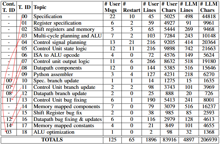
Restarts: Sometimes ChatGPT-4 outputs suboptimal responses. If so, the engineer has two options: (1) continue the conversation and nudge it to fix the response, or (2) use the interface to force ChatGPT-4 to ‘restart’ the response, i.e. regenerating the result by pretending the previous answer never occured. Choosing between these has trade-offs and requires professional judgement: continuing the conversation allows for the user to specify which parts of the previous response are good or bad, but regeneration will keep the overall conversation shorter and more succinct (valuable considering the finite context window size).
Still, as can be seen from the ‘# Restart’ column in the result table, the number of restarts tended to decrease as I grew more experienced with using ChatGPT-4, with Topics 00-07 having 57 restarts compared to Topics 08-18 having just 8. The highest individual number of restarts on a single message was 10, in Topic 04 (Control signal planning) which has the following message:
Click to expand
This looks excellent. According to this list, please produce the module definition for a control unit in Verilog which could operate the processor datapath. Please comment the purpose of each I/O. If a signal is for controlling a multiplexer, please also comment what each possible value should correspond to in the datapath.
This was a difficult prompt because it asks for a specific kind of output with a significant amount of detail, but eventually yielded a satisfactory answer as listed here:
Click to expand
module control_unit (
    // Clock input
    input wire clk,
    // Reset input
    input wire rst,
    // Input from the Instruction Register (IR)
    input wire [7:0] instruction,
    // Enables writing to the PC
    output wire PC_write_enable,
    // Selects the input for the PC multiplexer
    // 00: PC + 1 (FETCH cycle, BEQ_FWD, BNE_FWD)
    // 01: ACC (JMP, JSR)
    // 10: PC - 3 (BEQ_BWD, BNE_BWD)
    output wire [1:0] PC_mux_select,
    // Enables writing to the ACC
    output wire ACC_write_enable,
    // Selects the input for the ACC multiplexer
    // 00: ALU output
    // 01: Memory contents (LDA, LDAR)
    // 10: PC (JSR)
    output wire [1:0] ACC_mux_select,
    // Enables loading new instruction into IR from memory
    output wire IR_load_enable,
    // Control signal specifying the ALU operation
    output wire [3:0] ALU_opcode,
    // Selects input B for the ALU multiplexer
    // 0: Memory contents (ADD, SUB, AND, OR, XOR)
    // 1: Immediate (ADDI)
    output wire ALU_inputB_mux_select,
    // Enables writing to memory (STA)
    output wire Memory_write_enable,
    // Selects input for memory address multiplexer
    // 00: IR[4:0] (LDA, STA, ADD, SUB, AND, OR, XOR)
    // 01: ACC (LDAR)
    // 10: PC (Instruction fetching)
    output wire [1:0] Memory_address_mux_select
);
Bug repair: After errors were encountered, we would use ChatGPT-4 to repair them. An example of this is presented here. This is based on Conversation 15, and demonstrates how an error in the shift register primitive was resolved.
Click to expand
15 - SHIFT REGISTER BUG FIXUSER:
I have the following shift_register written in Verilog:
module shift_register #(
    parameter WIDTH = 8
)(
    input wire clk,
    input wire rst,
    input wire enable,
    input wire [WIDTH-1:0] data_in,
    output wire [WIDTH-1:0] data_out,
    input wire scan_enable,
    input wire scan_in,
    output wire scan_out
);

    reg [WIDTH-1:0] internal_data;

    // Shift register operation
    always @(posedge clk) begin
        if (rst) begin
            internal_data <= {WIDTH{1'b0}};
        end else if (enable) begin
            internal_data <= data_in;
        end else if (scan_enable) begin
            internal_data <= {internal_data[WIDTH-2:0], scan_in};
        end
    end

    // Output assignment
    assign data_out = internal_data;
    assign scan_out = internal_data[WIDTH-1];

endmoduleASSISTANT:
Sure! The issue arises from the part where you define the concatenation of the internal_data register when `scan_enable` is high. When the WIDTH is set to 1, the range `internal_data[WIDTH-2:0]` will cause an out-of-bounds access to the internal_data register.
To fix this, you can use a conditional expression to handle the case where WIDTH is set to 1. Here's the updated code:
module shift_register #(
    parameter WIDTH = 8
)(
    input wire clk,
    input wire rst,
    input wire enable,
    input wire [WIDTH-1:0] data_in,
    output wire [WIDTH-1:0] data_out,
    input wire scan_enable,
    input wire scan_in,
    output wire scan_out
);

    reg [WIDTH-1:0] internal_data;

    // Shift register operation
    always @(posedge clk) begin
        if (rst) begin
            internal_data <= {WIDTH{1'b0}};
        end else if (enable) begin
            internal_data <= data_in;
        end else if (scan_enable) begin
            if (WIDTH == 1) begin
                internal_data <= scan_in;
            end else begin
                internal_data <= {internal_data[WIDTH-2:0], scan_in};
            end
        end
    end

    // Output assignment
    assign data_out = internal_data;
    assign scan_out = internal_data[WIDTH-1];

endmoduleUSER:
Thanks! Can you also make it so scan_enable has a higher priority than the normal enable?
ASSISTANT:
Sure! To give the `scan_enable` signal a higher priority over the `enable` signal, you can change the order of the conditions in the always block. Here's the updated code:
module shift_register #(
    parameter WIDTH = 8
)(
    input wire clk,
    input wire rst,
    input wire enable,
    input wire [WIDTH-1:0] data_in,
    output wire [WIDTH-1:0] data_out,
    input wire scan_enable,
    input wire scan_in,
    output wire scan_out
);

    reg [WIDTH-1:0] internal_data;

    // Shift register operation
    always @(posedge clk) begin
        if (rst) begin
            internal_data <= {WIDTH{1'b0}};
        end else if (scan_enable) begin
            if (WIDTH == 1) begin
                internal_data <= scan_in;
            end else begin
                internal_data <= {internal_data[WIDTH-2:0], scan_in};
            end
        end else if (enable) begin
            internal_data <= data_in;
        end
    end

    // Output assignment
    assign data_out = internal_data;
    assign scan_out = internal_data[WIDTH-1];

endmodule(This bug fix worked too!)
The Developed Instruction Set Architecture (ISA)
Once again, all the chat logs are in our repository, this time in the free-chat-gpt4-tt03 folder.
The ISA co-generated with ChatGPT-4 in Conversation 00 (and updated in 10) is presented in the following table:
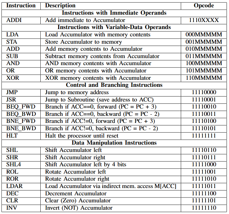
It is a relatively straightforward accumulator-based design with some notable features:
- given the size constraints, the memory-access `Instructions with Variable-Data Operands’ use just five bits to specify the memory address, meaning the processor would be limited to an absolute maximum of 32 bytes of memory.
- There is just one instruction with an immediate-data encoding.
- The instructions use the full 256 possible byte encodings.
- The JSR instruction makes it possible to implement subroutine calls, albeit a little awkwardly (there’s no stack pointer).
- The branch instructions are restrictive but useful. Skipping two instructions backwards allows for efficient polling (e.g. load an input, mask it for relevant bit, then check if 0 or not). Skipping 3 instructions forwards allows to skip over the instructions needed for a JMP or JSR. These were designed over a number of iterations, including a later modification (Conversations 10-12, the ‘branch update’) which increased the jump forwards from 2 instructions to 3 after during simulation I realized that we could not easily encode JMP/JSR in just 2 instructions.
- The LDAR instruction allows for pointer-like dereferences for memory loads. This enabled us to efficiently use a table of constants in our memory map (added in Conversation 17) to convert binary values into LED patterns for a 7-segment display.
When attempting to write programs in it, it feels like a variant of what might have been used for a PIC microcontroller family. ChatGPT-4 actually wrote the assembler for me as well, which I could have made better (it is truly awful to use, but it does work - See conversation 09).
I called the implementation for this processor the QTCore-A1 (cutie core).
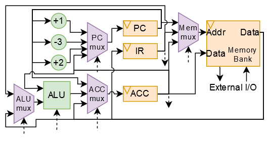
This is the datapath that eventually resulted (control signals are indicated with dotted lines - a moore-type multicycle FSM was used to control them). When designing the processor, I made sure that every register was also connected via a scan chain (also designed by ChatGPT-4!). This meant I could program the design once implemented, and it was also how I loaded my test programs during simulation.
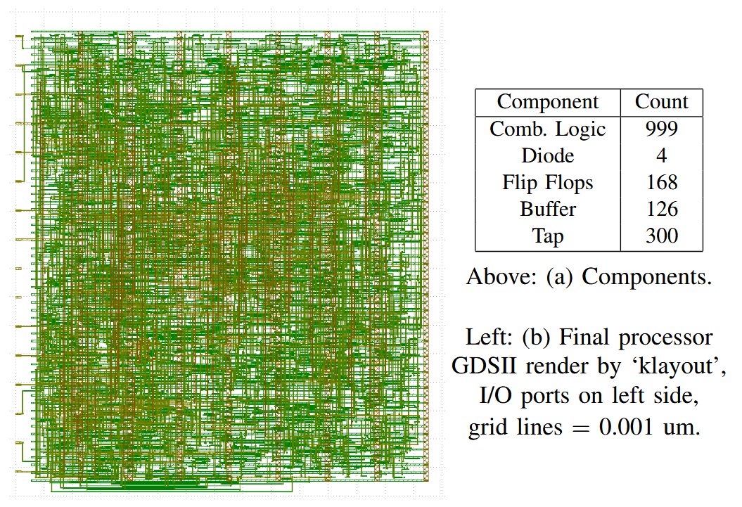
I tried to synthesize using OpenLane, but drat - the design would not fit in the 1000 standard cells! The easiest thing to do was to keep trimming the memory, which I did over and over again, until I eventually hit the magic number, and managed to get just 17 bytes of combined data and instruction memory. Yikes!
After synthesis by OpenLane, this is what the GDS looked like:
I wrote a few test programs, and soon realized I needed a few recurring constant values. After playing, I also realized that constant values in the memory map didn’t take up as much space as registers! So I managed to fit in a few constant helper values, including “1” and “0” into the memory map.
This meant I could write this little program in the cursed assembly language for a processor that I downloaded to an FPGA (CMod-A7) - although I also had to implement a programmer, which I did using an STM32! (Don’t mind the fact that this video is taken on a chair, I was literally building this in a conference theatre while attending a talk - the Tiny Tapeout deadline was fast approaching).
; this program tests the btn and LEDs
; after each BTN is low then BTN is high (i.e. a button release)
; it will toggle the LEDs between
; two values (matching blue and purple colors)
; BTNs and LEDS are at address 17, btn at LSB
0: LDA 17 ; load the btn and LEDS
1: AND 16 ; mask the btn
2: BNE_BWD ; if btn&1 is not zero then branch back to 0
3: LDA 17 ; load the btn and LEDS
4: AND 16 ; mask the btn
5: BEQ_BWD ; if btn&1 is zero then branch back to 3
;
; the button has now done a transition from low to high
;
6: LDA 14 ; load the counter toggle
7: XOR 16 ; toggle the counter using the btn mask
8: STA 14 ; store the counter value
9: ADDI 14 ; get the counter value offset (if 0, will be 14 (which is 0), if 1, 15)
10: LDAR ; load the counter LED pattern
11: STA 17 ; store the LED pattern
12: CLR
13: JMP ; returns to address 0
;
; data
;
14: DATA 0; toggle and LED pattern 0
15: DATA 24; LED pattern of ON (test for led_out=value 12, since 24>>1 == 12)
16: DATA 1 ; btn and counter mask
Here it is working!
So, I was happy, it worked in simulation and on an FPGA, so I happily sent it off to Tiny Tapeout, and then we released our paper to the arXiv and our design as open-source - you can take a look and if you have an FPGA, even have a play! Github link
Part 5: The Efabless Competition and the QTcore-C1
We received a lot of feedback on the submission. Matt Venn of Tiny Tapeout actually interviewed myself and Jason for his webinar! Youtube link, video embed below:
This went live 2 June 2023, and received a lot of attention (relatively)! We were also were contacted by a number of different companies in the EDA space including a few you have most definitely heard of.
One of the most interesting, though, was a call I ended up having with the good folks at Efabless, who told me that they had been planning an AI generated open-source silicon design challenge - and given that we had just performed such a feat, perhaps we should consider entering? The only wrinkle was that they were doing the contest at short notice, and we’d only have a few weeks to prepare - weeks in which I was actually overseas at a series of conferences!
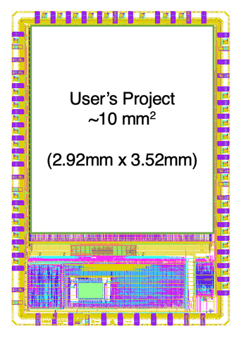
I decided that I would enter, but I would have to make some compromises. Their competition was based around the Efabless Caravel ChipIgnite platform, which pairs a RISC-V core with a user project area, such that you can design a hardware block with a wishbone connection and it will be placed alongside the core. This image, taken from the Efabless website, shows it best:
There was tons more space, but time was short. I would follow the methodology I’d previously laid out, and starting from the QTcore-A1, modify the microcontroller so that it was would take up the greater area available in the Efabless Caravel platform (it seemed like a tremendous shame to only use a fraction of the available space).
There were a few main wrinkles:
- although this was based on OpenLane, just like Tiny Tapeout, it was a much more manual and involved process, and there wasn’t a simple Github-actions based workflow. I had to install a lot of stuff to my laptop!
- The simulations needed to be a lot more robust than for Tiny Tapeout, and given that your design needed to be verified alongside the caravel core, it took much longer - my most basic simulation still took over 45 minutes, up from about 10 seconds for Tiny Tapeout.
- This was a competition, and the entries would be judged on how well they were documented, could be used, contribution to the open source, etc. So I had to also make sure everything was good on that front!
I decided I would make ChatGPT-4 make the following changes to the QTCore-A1. Firstly, the memory size would be upgraded to 256 bytes of shared instruction/data memory, divided into 16-byte pages. Secondly, I would add some peripherals - a 16-bit timer, some I/O ports, and given that I am a hardware security researcher in my day job, I also decided to add 2 eight-bit ‘memory execution protection’ control registers to provide ‘execution’ bits for each of the 16 pages, and update the original, cursed branch logic.
The new ISA:
As before, everything is provided open-source, but this time it is in the QTcore-C1 GitHub repository, under the AI_generation_information/chats folder. Each chat extends a conversation from the original QTCore-A1.
This was the ISA that ChatGPT eventually settled on when I prompted it with design chages.
Instructions with Variable-Data Operands
| Instruction | Opcode | Registers/Effects |
|---|---|---|
| LDA | 0000MMMM | ACC <= M[{Segment, MMMM}] |
| STA | 0001MMMM | M[{Segment, MMMM}] <= ACC |
| ADD | 0010MMMM | ACC <= ACC + M[{Segment, MMMM}] |
| SUB | 0011MMMM | ACC <= ACC - M[{Segment, MMMM}] |
| AND | 0100MMMM | ACC <= ACC & M[{Segment, MMMM}] |
| OR | 0101MMMM | ACC <= ACC | M[{Segment, MMMM}] |
| XOR | 0110MMMM | ACC <= ACC ^ M[{Segment, MMMM}] |
Immediate Data Manipulation Instructions
| Instruction | Opcode | Registers/Effects |
|---|---|---|
| ADDI | 1000IIII | ACC <= ACC + IMM |
| LUI | 1001IIII | ACC <= IMM « 4, ACC[0:3] <= 0 |
| SETSEG | 1010IIII | Segment <= IMM |
Control/Status Register Manipulation Instructions
| Instruction | Opcode | Registers/Effects |
|---|---|---|
| CSR | 10110RRR | ACC <= CSR[RRR] |
| CSW | 10111RRR | CSR[RRR] <= ACC |
Fixed Control and Branching Instructions
| Instruction | Opcode | PC Behavior/Effects |
|---|---|---|
| JMP | 11110000 | PC <- ACC |
| JSR | 11110001 | ACC <- PC + 1, PC <- ACC |
| HLT | 11111111 | Stop execution |
Variable-Operand Branching Instructions
| Instruction | Opcode | Operand | PC Behavior |
|---|---|---|---|
| BEQ | 1100SBBB | Sign + Offset | If ACC == 0, PC <- PC ± Offset |
| BNE | 1101SBBB | Sign + Offset | If ACC != 0, PC <- PC ± Offset |
| BRA | 1110SBBB | Sign + Offset | PC <- PC ± Offset |
Data Manipulation Instructions
| Instruction | Opcode | Register Effects |
|---|---|---|
| SHL | 11110110 | ACC <- ACC « 1 |
| SHR | 11110111 | ACC <- ACC » 1 |
| ROL | 11111000 | ACC <- (ACC « 1) OR (ACC » 7) |
| ROR | 11111001 | ACC <- (ACC » 1) OR (ACC « 7) |
| LDAR | 11111010 | ACC <- M[ACC] |
| SETSEG_ACC | 11111011 | Segment <- ACC[3:0] |
| DEC | 11111100 | ACC <- ACC - 1 |
| CLR | 11111101 | ACC <- 0 |
| INV | 11111110 | ACC <- ~ACC |
The datapath:
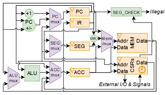
Whew, a lot of changes in there! Observe there is now the segment register which is concatenated with parts of the instructions to decode the addresses for instructions with variable data operands.
Here’s the full details:
- Control Unit: 2-cycle FSM for driving the processor (3 bit one-hot encoded state register)
- Program Counter: 8-bit register containing the current address of the program
- Segment Register: 4-bit register containing the current segment used for data memory instructions
- Instruction Register: 8-bit register containing the current instruction to execute
- Accumulator: 8-bit register used for data storage, manipulation, and logic
- Memory Bank: 256 8-bit registers which store instructions and data.
-
Control and Status Registers: 8 8-bit registers which are used for special features including the timer, I/O, memory protection, and sending an interrupt and receiving and sending signals to the larger Caravel processor.
- Control/Status Registers (CSRs) and their addresses
-
SEGEXE_L (000): 8 bits - Represents the lower half of the memory segments that are designated as executable. Each bit in the register corresponds to a segment in the lower half of memory space. If a bit is set to 1, the corresponding segment is marked as executable.
-
SEGEXE_H (001): 8 bits - Represents the higher half of the memory segments that are designated as executable. Each bit in the register corresponds to a segment in the upper half of memory space. If a bit is set to 1, the corresponding segment is marked as executable.
-
IO_IN (010): 8 bits - Input register for UART (or any general I/O device) operations. This is used to read data from external devices.
-
IO_OUT (011): 8 bits - Output register for UART (or any general I/O device) operations. This is used to write data to external devices.
-
CNT_L (100): 8 bits - Lower 8 bits of a 16-bit counter register. This can be used to store the lower half of a count value, which could be used for timing operations, or looping in programming, etc.
-
CNT_H (101): 8 bits - Higher 8 bits of a 16-bit counter register. This can be used to store the upper half of a count value, similar to the CNT_L register.
-
STATUS_CTRL (110): 8 bits - A control register to hold the status of different operations in the CPU. The bits are:
{SIG_OUT[7:2], CNT_EN[1], IRQ_OUT[0]}. The SIG_OUT bits are used to send signals (6 bits) to the larger Caravel processor. The CNT_EN bit is used to enable the counter. The IRQ_OUT bit is used to send an interrupt to the larger Caravel processor. -
SIG_IN (111): 8 bits - The 8-bits here can come from the larger Caravel processor. This can be used to send signals to the CPU, such as job start, job end, etc.
Example programming using the assembler
Writing assembly programs for QTCore-C1 is simplified by the assembler produced by GPT-4.
Presenting programs to the assembler:
- Programs are presented in the format
[address]: [mnemonic] [optional operand] - There is a special meta-instruction called DATA, which is followed by a number. If this is used, just place that number at that address.
- Programs cannot exceed the size of the memory (in QTCore-C1, this is 256 bytes).
- The memory contains both instructions and data.
Example program:
In this program observe how we read and write to the I/O, the timer, and the data memory via SETSEG. We also set the memory segments to be executable via CSW, and then jump to a non-executable segment to crash the processor.
Click here for program
; this program tests the IO and counter registers via (CSR/CSW) and the interrupt emitter
; it should crash with a HALT after jumping to a non-executable data segment
; check output: program halted
; check output: IO_OUT = 15
; check output: M[240] = IO_IN
; check output: M[253] = 2
; check output: M[254] = 0b11111101
; check output: M[255] = 0xf1
0: CLR
1: SETSEG 15
2: LDA 0 ; loads value M[16*15 + 0 = 240] = 15
3: CSW 3 ; sets the value 15 to the CSR register 3 (IO_OUT)
4: CSR 2 ; reads from CSR register 2 (IO_IN) to ACC
5: STA 0 ; sends the IO_IN value to M[16*15 + 0 = 240]
6: CLR ;
7: ADDI 15;
8: CSW 0 ; sets SEGEXE_L to 0x0F, making just segments 0-3 executable
9: CSW 1 ; sets SEGEXE_H to 0x0F, making just segments 8-11 executable
10: CLR ;
11: LDAR ; loads the value of M[0] = 0b11111101 into ACC
12: STA 14; stores it in M[16*15 + 14 = 254]
13: CLR ;
14: CSW 4; set 0 to CNT_L
15: CSW 5; set 0 to CNT_H
16: ADDI 2;
17: CSW 6; set the second bit of STATUS_CTRL (starts the counter)
18: ADDI 0; timer to value 1
19: CSR 4; reads the timer (value = 1), timer to value 2
20: CSR 4; reads the timer (value = 2), timer to value 3
21: STA 13; stores it in M[16*15 + 13 = 253] (should be value 2)
22: LUI 3;
23: JMP ; jumps to address 48

48: CLR ;
49: LUI 15;
50: ADDI 1; make the constant 0xf1
51: STA 15; store it in M[16*15 + 15 = 255]
52: JMP; jumps to address 0xf1 (241)

240: DATA 15
241: CLR ; sets ACC to 0, but actually we should crash here for being non-executable
242: JMP
You can see all the other juicy details at the QTcore-C1 GitHub.
Part 6: Receiving the silicon
Well, we entered the contest (submission was finally finalized 2 hours before the deadline at 6am on the due morning), and - the QTcore-C1 won, woohoo! This meant that the chip would get taped out, and I would get copies of the silicon in the mail!
I did a webinar with Efabless afterwards, on how the process works, my motivation, and how you can get started in this area as well - Youtube link, embedded video below:
I then joined their panels as a judge for the second and third iterations of the contest.
And then, just two weeks ago, I got a parcel in the mail, and…
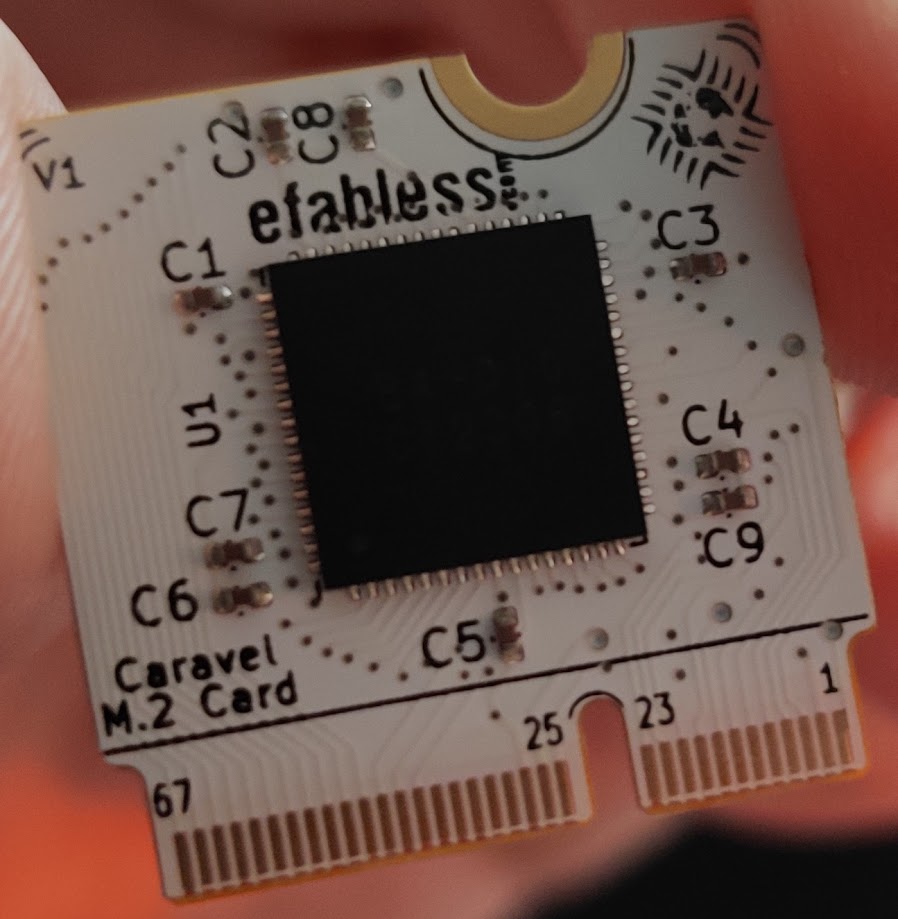
It had arrived! (To be precise, I received ten chips on these little carrier boards, and fifty chips which I have to solder myself!)
Part 7: Basic tests and a christmas LED display!
The first thing I needed to test was that I could actually talk to my chip, just as I had been able to do in the simualations. I spun up the program I had made for the original competition deadline, and put it into the Caravel, then realized that it “passed” only according to the simulator inspecting values - i.e. the processor did not actually emit anything! So I had to update the RISC-V program to have UART, which was thankfully quite easy thanks to the caravel documentation.
After one devastating experiment where nothing happened and I thought the chip didn’t work, I realized I needed to do one extra configuration step to enable the caravel userspace wishbone bus, and then I ran the program, and -
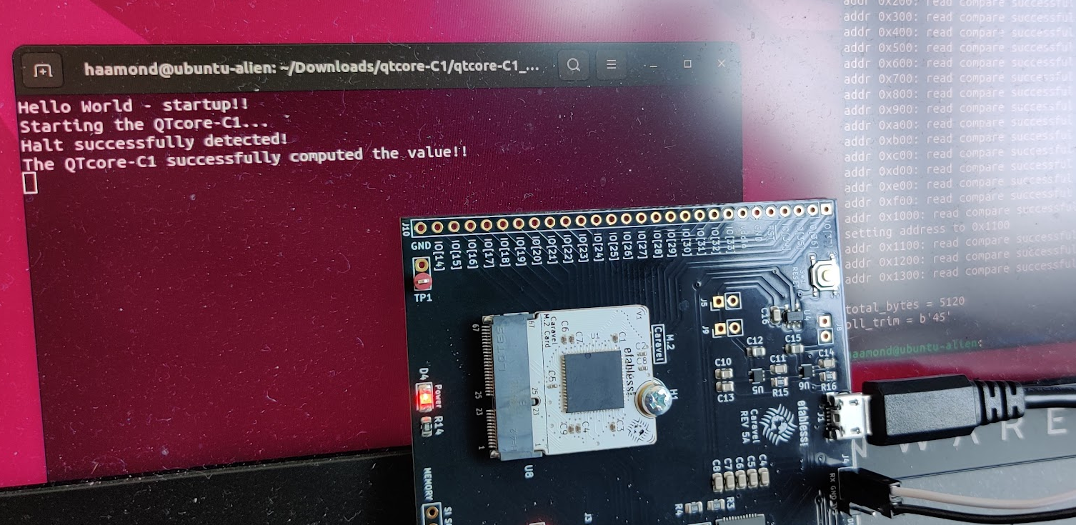
It works!
It’s hard to describe how amazing it felt to have a working piece of silicon in front of me that I had taken a part in designing, especially since I had never actually designed anything taped out before. Nor, perhaps, would I have done, without LLMs like ChatGPT to inspire me to try.
I did a few more experiments, and found that there are perhaps some issues with the chip, including an issue where it doesn’t want to restart after running a HALT command (annoying since I like to HALT to indicate a program has finished running!).
I ended up creating a simple counter program with a handshake to the caravel processor, similar to the LED blinking program, from earlier, and then - tada - the festive, christmas tree extravaganza:
What’s next?
I have worked with LLMs for hardware since 2020 because I believe that they have an enormous potential to simplify, democratize, and accelerate hardware development, especially when used in conjunction with open-source design flows like that provided by OpenLane and Caravel.
I don’t think I am alone in this view, either. In recent months, RapidSilicon has announced RapidGPT, NVIDIA has brought out ChipNeMo, Cadence announced JedAI, and Synopsys.AI has launched. All of these are real-world commercial enterprises which aim to bring LLMs into the hardware space.
I’m really excited for what comes next.
And as for me, I’ll keep tinkering - I’ve definitely got some more experiments I want to run and more places I can see LLMs being useful in hardware design!