I was cycling through a light industrial area in Auckland City when I came across a rubbish bin awaiting pickup on the side of the road. It caught my eye as it was practically overflowing with discarded LED Matrix modules - big ones, about a foot in each dimension! I couldn’t believe it - firstly, discarding e-waste in a manner such as this is actually illegal in New Zealand. Secondly, the LED modules - for the most part - actually looked to be in pretty good condition! I grabbed as many as I could carry on the bike and carried on home, keen to see if I could get them going!
Note: All work used in this blog post is published on my Github.
Second note: After I posted this to Reddit, user /u/dakesew identified the protocol as a subset of Hub75, discussed further at the end of this post.
First impressions
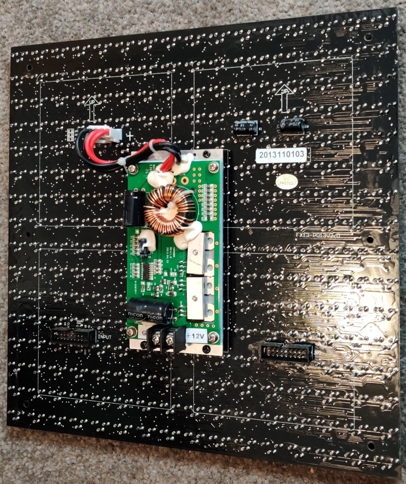
Here are pictures of the front and back of one of the LED modules.
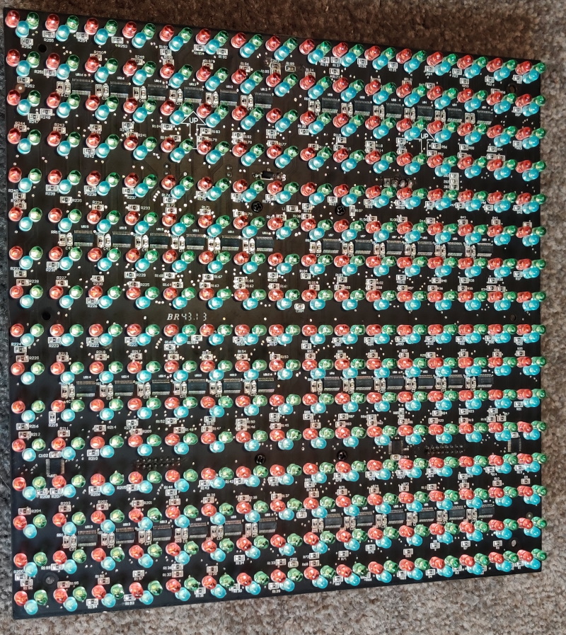
Straight away we can see several interesting pieces of information.
- The modules have a well-labelled 12V power supply input
- The modules appear to have an INPUT port and an OUTPUT port, presumably for data
- There is a part number ‘FX13-P013V2.0’, or possibly ‘BR43.13’. Unfortunately, neither of these part numbers return anything on Google.
- There is what could be a date from 2013 on a sticker (although it has 2 digits too many?), as well as a QC passed label
The input port is interesting:
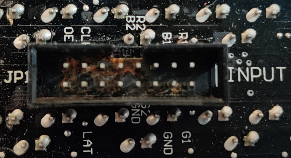
Thanks to the labels (Whoever designed this PCB, seriously, thanks) this gives us some idea of how these modules might be controlled. ‘GND’ are grounds, ‘OE’ is almost certainly ‘output enable’, ‘CLK’ is a clock which implies a serial control scheme of some kind, ‘LAT’ is probably short for ‘latch’, and R1/R2/G1/G2/B1/B2 are likely the colour inputs.
I paused at this point for dinner, and flicked a message to a former colleague that used to work at a tech company involved in digital road signs (among other things), asking him if there was a standard control scheme for LED modules such as these. He said that usually they were designed upon standard shift registers - direct quote “The modules are usually dumb, intelligence is in the controllers”.
So, once I got back, I took a closer look at the ICs that were stamped around the board - I found only two kinds.
- Located near the INPUT and OUTPUT ports are 74HC245 chips. These are ‘Octal Bus Trancievers’ and appear to be being used as I/O protection.
- Located between groups of LEDs are MBI5024 chips. Looking these up online, they are Shift Registers designed for use in applications such as LED boards - fancy that! This also gives credence to my former colleague’s theory - it sure seems like we’ll just need to shift in data to display it.
I recreate the block diagram for the MBI2054 here:
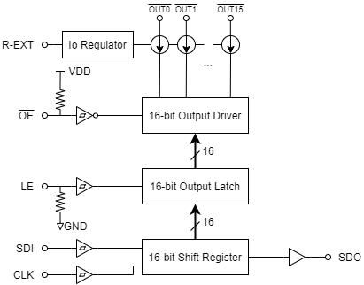
We can also get the following helpful information out of the data sheet:
| Port | Function |
|---|---|
| SDI | Serial-data input to the internal shift register |
| CLK | Clock input terminal. Data shifts in on a rising edge |
| LE | Data strobe input terminal. Serial data is transferred to the output latch when LE is high, and the data is latched when LE is low. |
| nOE | Output enable terminal (active low). When low, the output drivers are enabled, when high, output drivers are disabled. |
As a refresher or in case you’re unfamiliar, shift registers operate according to the following generic internal block diagram:
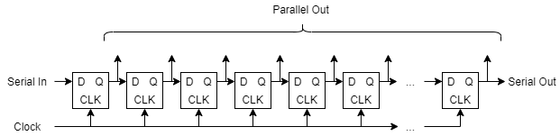
Each of the boxes in this diagram is a D type Flip Flop. On a rising clock edge, they capture the data at D, to be then emitted at Q. As such, after the first clock tick, the first flip flop will be emitting the first bit of data from the serial input. You then change the serial input to the next bit of data, and pulse the clock again. Now, the first flip flop is outputting the second bit of data, and the second flip flop is outputting the first. On and on this goes until you completely fill your shift register, and your input data stream is now present on the outputs of the shift register in parallel.
From the datasheet then, we can conclude that inputs LAT, CLK, and OE are going to all shift registers in parallel. Presumably then the R1/R2/G1/G2/B1/B2 are the data inputs to the shift registers. Why, though, are there two wires for each?
Investigations with a microcontroller
It’s worth pointing out here that due to the coronavirus outbreak, at the time of performing this work, I was stuck at home without my usual work-provided equipment and components. At any rate, I figured that I could probably get away with what I had on hand. Firstly, I needed to make sure I could safely power up the LED module. I found a 12V 2A power supply, and applied it. Then, I pulled the OE pin low, and brushed noise against the LAT, CLK, and data pins. Every LED abruptly turned on - I had invited the sun into my office. These boards are hecking bright! Fortunately, nothing exploded or melted. A good start! Using a multimeter, I could see that my 12V power supply output had dropped to 11.5V, so I turned everything off.
My first experiment was to find out (a) how the loaded data made its way to pixels on the screen, (b) the purpose of the two pins for each colour, and (c) how much current this board was actually trying to draw. Unfortunately for me, my multimeter ammeter had a blown fuse, and I couldn’t go get another fuse from anywhere.
Fortunately, I had an Atmel Xplained Mini board (Atmega328PB based) at home to work with, so I used this as my controller. I quickly wrote a small program to bit bash out data to the shift register’s G1 pin (chosen at random). I was interested to see what would happen if I pumped different data into the system.
//Note: this will only control one bit of R1/R2/G1/G2/B1/B2, all others are forced to zero.
//(i.e. this is not suitable for actual use, just for experimentation)
void Disp_Send(uint8_t val, uint8_t color_pin) {
	//for each bit in val
	for(int i=0; i < 8; i++) {
		//put the i-th bit onto the color_pin pin
		PORT_MATRIX_COLORS = 0;
		if((0x80 >> i) & val) {
			PORT_COLORS |= (1 << color_pin);
		}

		//now toggle the CLK pin to store the bit
		_delay_us(1); //first delay is for settling time
		PORT_MATRIX_CTRL |= (1 << PIN_CLK);
		_delay_us(1);
		PORT_MATRIX_CTRL &= ~(1 << PIN_CLK);
	}

	//now latch the output by toggling the LAT pin
	_delay_us(1); //first delay is for settling time
	PORT_MATRIX_CTRL |= (1 << PIN_LAT);
	_delay_us(1);
	PORT_MATRIX_CTRL &= ~(1 << PIN_LAT);
}
I had it wired as follows:
//CLK and LAT are on PORT C
#define DDR_MATRIX_CTRL DDRC
#define PORT_MATRIX_CTRL PORTC
#define PIN_CLK 0
#define PIN_LAT	1

//OE is associated with PORT B3 as this goes with PWM for TIMER2 (OC2A pin is same pin as PB3)
#define DDR_MATRIX_OE DDRB
#define PORT_MATRIX_OE PORTB
#define PIN_OE 3

//color pins on PORT D
#define DDR_MATRIX_COLORS DDRD
#define PORT_MATRIX_COLORS PORTD
#define PIN_R1 0
#define PIN_R2 1
#define PIN_B1 2
#define PIN_B2 3
#define PIN_G1 4
#define PIN_G2 5
And here’s a clearer representation of that INPUT port from earlier:
INPUT PORT, TOP DOWN VIEW
+------------------+      +------------------+
|                  +------+                  |
|                                            |
| OE   CLK   NC   NC    B2    R2    B1    R1 |
|                                            |
| NC   LAT   NC   NC    GND   G2    GND   G1 |
|                                            |
+--------------------------------------------+
In the main(), I simply called Disp_Send(0xFF, PIN_G1) with a short delay over and over again in a loop.
To prevent cooking my power supply and further searing of my eyeballs, I also configured the OE pin as a PWM, keeping the display on only 6.25% of the time (16 cycles of every 256).
I grabbed one of the other LED modules now, one which was missing several LEDs on the PCB, so that if something went wrong I wouldn’t break one of the modules that appeared to be in better condition. I was able to see data coming onto the screen! I modified the code slightly to use both pins 1/2 of each color, and then produced the following output:
Brilliant! It seems that the R1/G1/B1 refer to the shift registers controlling the top 8 rows, and the R2/G2/B2 refer to the shift registers controlling the bottom 8 rows.
Examining power requirements
During all of this I had let a good friend know about the rubbish bin full of LED modules. He took a spin out in his car to get some for himself, and sent me some maths about the LEDs:
LED Datasheet says that they're 18mA.
There's 16x16x3 LEDs, times that by 18ma, that's 13A overall.
The PSU on the back of each module outputs 5V, so that's 69W.
If we divide that by the 12V in, that's 5.67A at 12V.
A good point, and one I should have considered earlier. He then measured it using a better power supply than I have at home, and measured 3.7 A given 13V input (~48W). The maths was an overestimate then, but it confirmed that I still needed to be careful in my code - keeping the display at 6% PWM seemed sensible.
Although, we then got curious, so I wound it back to full brightness, and hooked up an old oscilloscope across the power pins of my PSU:
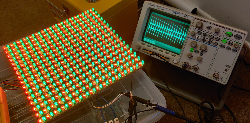
It looked like my power supply was not, in fact, coping - those spikes were around 4V in size!
My friend then sent me this image, after he’d got invested in disassembling one of his LED modules:
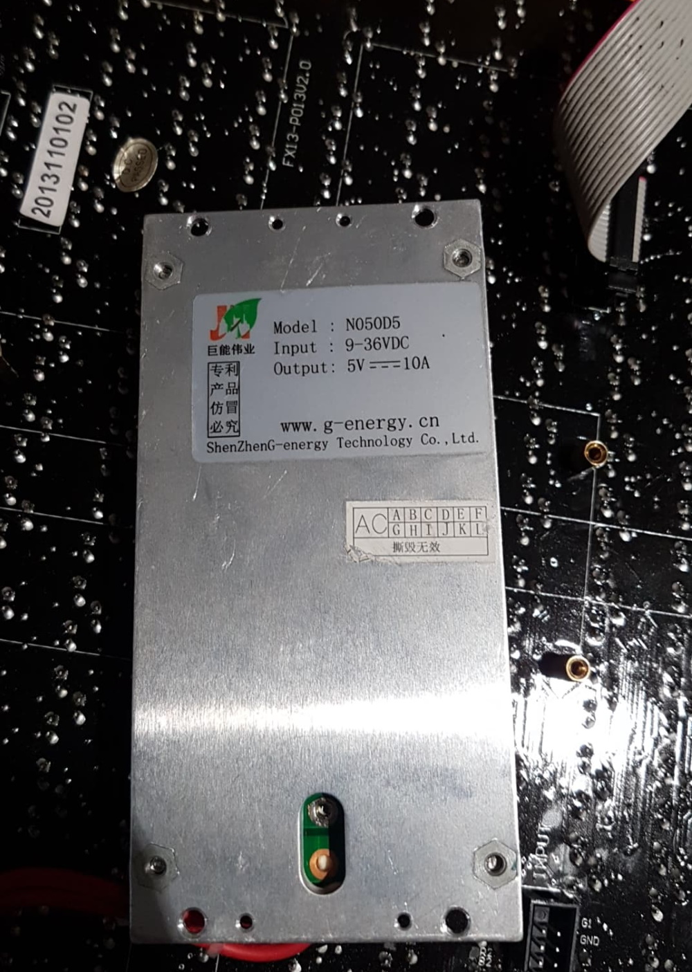
Turns out these modules can take up to 36V! I immediately switched over to a different PSU I had at home, one that was 24V 2A, which should just cope with the ~48W he measured earlier. I found with my oscilloscope that at full brightness (which was now even brighter than before), the 24V 2A PSU gave an average of 24.3V, with a 1Vpp oscillation at about 50kHz. Hence, it was still being overloaded, but not by as much.
At any rate, once I re-applied the PWM, the noise completely vanished, and the PSU was rock solid at 24V. I then took this opportunity to test all of the modules I grabbed (I had taken 8) - six of them worked perfectly with no dead pixels, two of them had a few dead and missing LEDs.
Display Matrix Layout
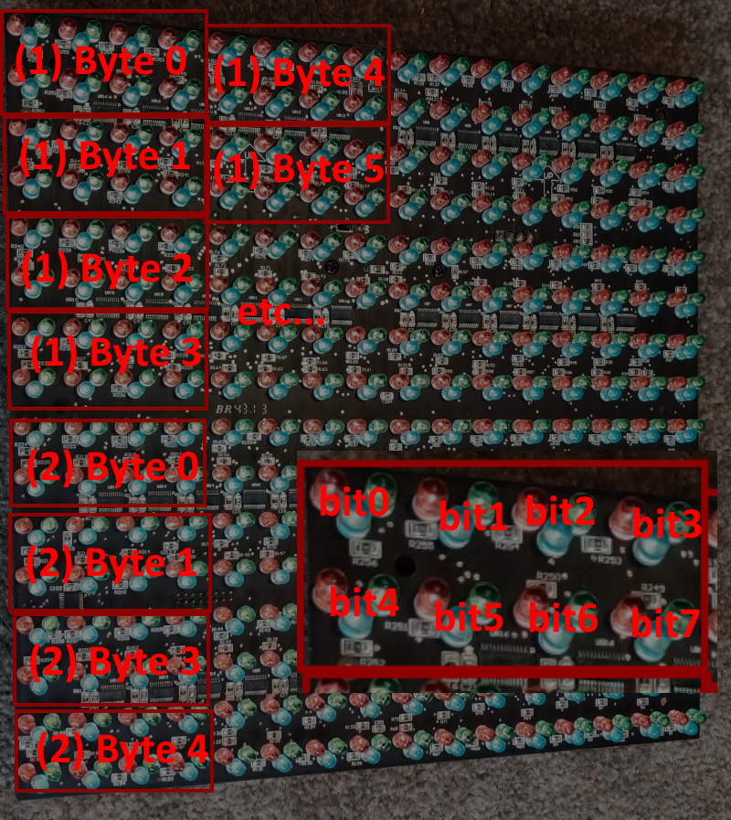
Satisfied we’d solved the power requirements, I now moved on to writing a basic algorithm to drive the display. From the experimenting earlier, I knew that the shift registers were arranged such that each eight bits of data was arranged in two four-bit rows. This cascaded down for four times in total, before the shift registers moved to the next segment. You can see this in the video from earlier in this write-up. I depict it here in this image:
So, all pixels are individually addressable, but getting them out is a little fiddly. Imagine you have a canvas of 16 pixels by 16 pixels. You address it as such:
px[16*16] =
+-----+-----+-----+-----+-----+ ... +-----+
|   0 |   1 |   2 |   3 |   4 |     |  15 |
+-----+-----+-----+-----+-----+ ... +-----+
|  16 |  17 |  18 |  19 |  20 |     |  31 |
+-----+-----+-----+-----+-----+ ... +-----+
:     :     :     :     :     :     :     :
+-----+-----+-----+-----+-----+ ... +-----+
| 239 | 240 | 241 | 242 | 243 |     | 255 |
+-----+-----+-----+-----+-----+ ... +-----+
To shift in this canvas to display it, you need to do the following:
- The shift registers are wired such that we output 4 pixels in a row, then the 4 pixels beneath them, then the 4 pixels beneath them… until 7 rows down, then we shift over one segment and repeat, i.e.
Send px[0], px[1], px[2], px[3], <-- first row, first 4 columns, px[16], px[17], px[18], px[19], <-- second row, first 4 columns, px[32], px[33], px[34], px[35], <-- third row, first 4 columns ... px[112], px[113], px[114], px[115], <-- eighth row, first 4 columns, THEN px[4], px[5], px[6], px[7], <-- first row, second 4 columns, px[20], px[21], px[22], px[23], <-- second row, second 4 columns, etc. - In addition, you need to remember that the bottom 8 rows are wired in parallel to the top 8 rows - so at the same time you send px[0], you also need to send px[128], and the same time you send px[1] you send px[129], and so on. (128 is 16*8, i.e. half the height of the px array).
I now put together some code to do this. Firstly, we define a color type, and two arrays to use as screen buffers:
typedef uint8_t pixel_color_t; //let's plan to use 8 bits for each pixel, format R  R  R  G  G  G  B  B

static volatile pixel_color_t scrbuf1[DISPLAY_WIDTH*DISPLAY_HEIGHT] = {0};
static volatile pixel_color_t scrbuf2[DISPLAY_WIDTH*DISPLAY_HEIGHT] = {0};

volatile pixel_color_t* frontbuf; //currently being rendered
volatile pixel_color_t* backbuf; //currently being manipulated

void Display_Init() {
	frontbuf = scrbuf1;
	backbuf = scrbuf2;
}

void Display_SwapBuffers() {
	if(frontbuf == scrbuf1) {
		frontbuf = scrbuf2;
		backbuf = scrbuf1;
	} else {
		frontbuf = scrbuf1;
		backbuf = scrbuf2;
	}
}
Why do we need two buffers? This is because displaying an array and drawing to an array should be mutually exclusive activities. Consider a screen that updates at 60Hz. No matter what, it needs to be able to send a picture out every ~16.6ms. But what if you haven’t finished setting up this frame’s picture yet? Drawing your pretty picture to a display is only practical if you aren’t currently halfway through updating it!
As such, we define a “front buffer” as the one that is currently being rendered by the system, and a “back buffer” as one that we’re currently manipulating, adding text and drawing shapes and so on. When we’re ready to swap them out, we change the pointers by calling Display_SwapBuffers.
Now, let us examine Display_TransmitBuffer(), which we shall call from within a timer interrupt (I used Timer0, set to 16ms, giving 62.5Hz update cycle for the display).
void Display_TransmitBuffer() {
	//1. Emit the screen buffer, pixel by pixel, into the shift registers.
	//Note: getting everything out in the right order is a chore
	//the shift registers are wired such that we output 4 pixels in a row, then the 4 pixels beneath them, then the 4 pixels beneath them... until 7 rows down,
	//then we shift over one segment and repeat
	//0  1  2  3   /
	//16 17 18 19  /
	// ....
	//4  5  6  7   /
	// etc.
	//Then, to make it slightly more complicated, we need to do the bottom 8 rows at the same time as the top 8 rows.
	//That is, the top and bottom 8 rows are loaded in parallel.
	//We call each pixel as we do this as px1 and px2 going to rgb1 and rgb2.

	//Whew! Overall, we get it all out with the following triple nested for loop:
	for(uint8_t seg = 0; seg < 4; seg++) {						//for each segment of 4 columns
		for(uint8_t row = 0; row < DISPLAY_HEIGHT/2; row++) {	//for each 8 rows in the segment
			for(uint8_t col = 0; col < 4; col++) {				//for each column in the 4 columns

				pixel_color_t px1 = frontbuf[seg * 4 + col + DISPLAY_WIDTH*row];		//convert (seg, col, row) to pixel address for the top 8 rows
				pixel_color_t px2 = frontbuf[seg * 4 + col + DISPLAY_WIDTH*row + DISPLAY_WIDTH*DISPLAY_HEIGHT/2];	//now add 128 to that and you have the pixel in the bottom 8 rows as well

				uint8_t r1 = (px1 & 0b11100000) >> 5; //extract rgb for px1
				uint8_t g1 = (px1 & 0b00011100) >> 2;
				uint8_t b1 = (px1 & 0b00000011);

				uint8_t r2 = (px2 & 0b11100000) >> 5; //extract rgb for px2
				uint8_t g2 = (px2 & 0b00011100) >> 2;
				uint8_t b2 = (px2 & 0b00000011);

				//load rgb onto output pins for px1 and px2
				//(while the format is RRR GGG BB, currently we ignore the intensity - as long as the value is >0, the LED will be on)
				if(r1) {
					PORT_MATRIX_COLORS |= (1 << PIN_R1);
				} else {
					PORT_MATRIX_COLORS &= ~(1 << PIN_R1);
				}
				if(r2) {
					PORT_MATRIX_COLORS |= (1 << PIN_R2);
				} else {
					PORT_MATRIX_COLORS &= ~(1 << PIN_R2);
				}
				if(g1) {
					PORT_MATRIX_COLORS |= (1 << PIN_G1);
				} else {
					PORT_MATRIX_COLORS &= ~(1 << PIN_G1);
				}
				if(g2) {
					PORT_MATRIX_COLORS |= (1 << PIN_G2);
				} else {
					PORT_MATRIX_COLORS &= ~(1 << PIN_G2);
				}
				if(b1) {
					PORT_MATRIX_COLORS |= (1 << PIN_B1);
				} else {
					PORT_MATRIX_COLORS &= ~(1 << PIN_B1);
				}
				if(b2) {
					PORT_MATRIX_COLORS |= (1 << PIN_B2);
				} else {
					PORT_MATRIX_COLORS &= ~(1 << PIN_B2);
				}

				//now toggle the CLK pin to store the rgb1 and rgb2
				_delay_us(1); //first delay is for settling time
				PORT_MATRIX_CTRL |= (1 << PIN_CLK);
				_delay_us(1);
				PORT_MATRIX_CTRL &= ~(1 << PIN_CLK);

				//rinse and repeat!
			}
		}
	}

	//2. Now all data is loaded, latch it to the outputs by toggling the LAT pin
	_delay_us(2); //first delay is for settling time
	PORT_MATRIX_CTRL |= (1 << PIN_LAT);
	_delay_us(2);
	PORT_MATRIX_CTRL &= ~(1 << PIN_LAT);
}
We then add a function to add pixels and lines, and can generate the following output:
From here, it also isn’t hard to add support for further features, e.g. text, circles, etc. I also modified the code so that it can support daisy-chained modules in the horizontal direction!
If you’re interested, the code that I wrote to do all of this is on the project Github under display.c
Can I try or use this myself?
In terms of the code, sure! Everything I’ve written is released on the Github project under the MIT license. In terms of the hardware, well, I couldn’t find the modules online anywhere, but presumably other modules with similar I/O requirements exist?
At any rate, thanks for reading - hopefully you found it interesting!
Community input
I posted this to Reddit if you’d like to comment! Already, user /u/dakesew identified the protocol as a subset of Hub75, which is a protocol designed for control of large RGB LED panels (often 32x32 or 16x32). The complete protocol mentions usage of the four grouped pins I marked as NC in the middle connector, calling them A/B/C/D, and mentioned that they are used for row addressing. On my panels they do not seem to be connected, however. Perhaps this is because my panels have fewer pixels (16x16), and/or the protocol was adopted incorrectly for this design.