Recently I purchased some Raspberry Pi Pico modules. This is blogpost #2 on the subject, where I will walk through a basic development board that I designed to be used to familiarise myself with the new RP2040 silicon.
In the rest of the blog post I’ll have a yarn. If you’re just interested in the Kicad files, you can get them here.
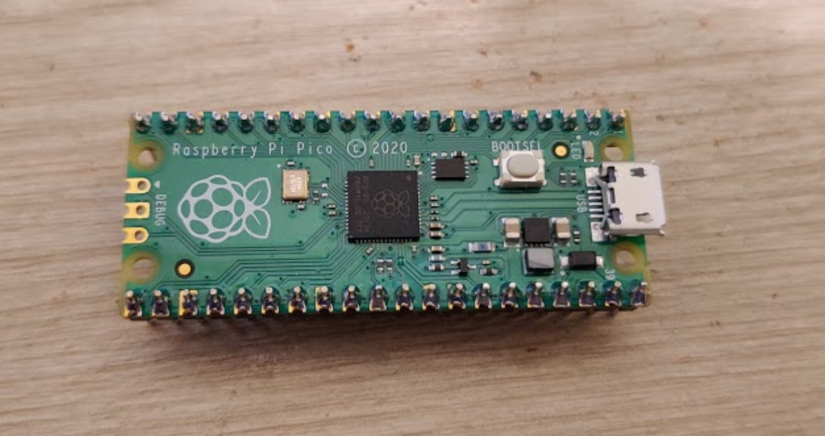
The Raspberry Pi Pico
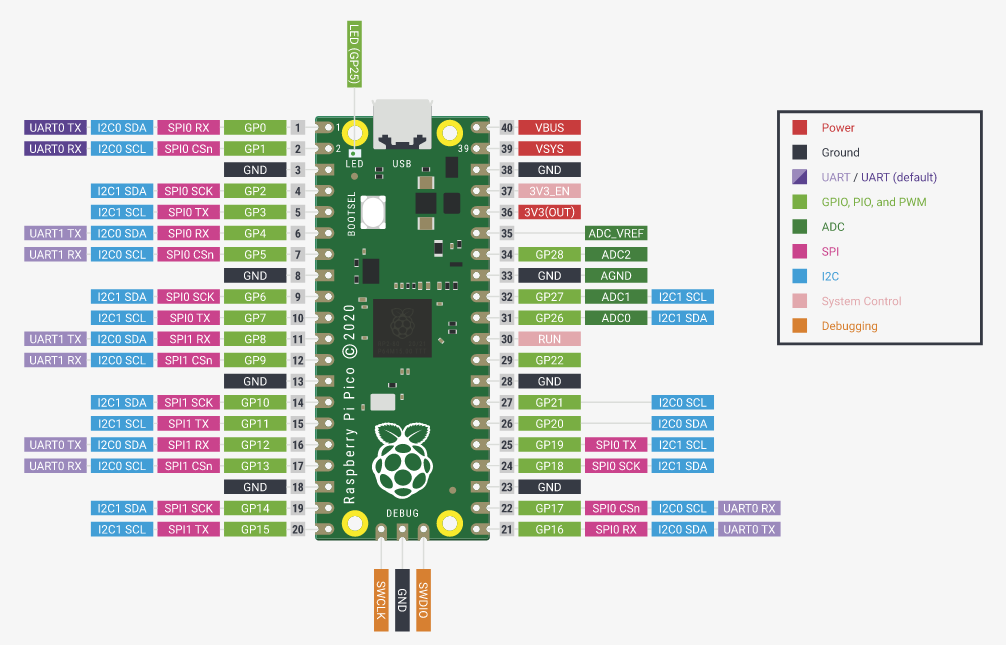
The Pico module has a very accessible footprint from a hobbyist point of view. With 20 pins down each side, and standard 2.54mm spacing, it’s both a reasonably small package while remaining quite comprehensive in its functionality.
I began by building on a breadboard, with echoes of nostalgia coming from my memories (I began my whole embedded journey as a nerdy teenager playing with PIC microcontrollers and breadboards).
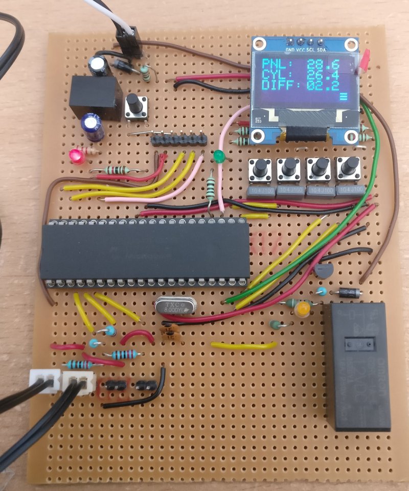
I also played with a lot of veroboard. A lot. For example, this board, one of my first:

Actually, I shouldn’t lie, it was only 2019 that I was still having fun building with PICs and playing with veroboard… and the PIC16F877A actually has the same footprint as a Pico module!
(Getting an SSD1306 to work with a PIC was its own challenge…)
Anyway, I remembered that I hate breadboards - I hated them as a teenager as well.
However, while as a teenager my financial and construction options were limited (veroboard was the absolute best I could muster) nowadays we have the wonders of fast and cheap online prototyping services. If you can stick to 10cm x 10cm 2 layer boards, all the major services can fabricate at extremely low cost.
So, I figured - why not take this opportunity to design myself a basic little board for the Pico?
The KIWIKIT Pico Baseboard
I decided quickly that I wanted to emulate the fun that I had growing up with DIY development kits, and so that meant (a) I was going to solder this myself (a bold choice since I am a Bad Solderer), and (b) I was going to use only through-hole components.
I also wanted to take the opportunity to clear out some of my component drawers rather than buy any components (how’s that for design space exploration). This meant I had to balance the axis of design complexity against dev kit usefulness. Overall, I ended up with the following shortlist:
- Two general purpose LEDs and a power LED (Rationale: I never regret having the ability to blink LEDs when getting started with a new chip, and the Pico module itself has no power LED).
- Three general purpose switches and a reset switch (Rationale: Similar to the above, switches are general purpose and very handy for most development boards, and the Pico module itself has no reset switch).
- An SSD1306 OLED (Rationale: Screens are both fun to play with and a good way to test the performance of a chip/your software skills).
- An AT24C08 EEPROM (Rationale: Harder to justify for a general purpose board, especially when the Pico has 2MB of onboard flash compared to the 1KB of potential EEPROM, but I have a ton of these floating around in DIP-8 packages which I purchased for 10 cents a chip in a fire sale on Digikey. Plus, the screen is already using one of the I2C busses so they can share).
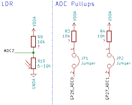
- An LDR on one of the ADC lines (Rationale: Gives me an easy-to-play-around-with analog input).
- Breakout pins for an SPI, arranged in the order present on cheap SD card modules (Rationale: I have 24 of these modules that I was given once, and I have to use them up somehow).
- Breakout pins for an I2C, arranged in the order present of cheap MP-6050 accelerometer/gyroscope modules (Rationale: I want to play with one of these modules).
- Breakout pins for the other 2 ADCs, with optional pullups (Rationale: Flexible and in a useful form factor: I have a couple of thermistors on long cables that could be plugged in).
- Breakout for every other pin (Rationale: don’t want to waste anything - gotta send them somewhere).
- Breakout for power (Rationale: Flexibile power sinking and sourcing options).
Having sorted this exhaustive list, I now got onto the design stage!
Putting it together with Kicad
In my opinion, Kicad is one of the best free/open source software projects in existence. Across its 20 years of development it has really matured into a real contender when it comes to PCB design. As such, I use it for basically all of my projects (both hobbyist and in work).
This isn’t meant to be a tutorial for Kicad, so I’ll just go through a few design choices.
In the schematic
Just as you can have well-organised and well-commented code, you can also have well-organised and well-commented schematics! Too often I am going through circuits wondering WTF something is doing. So, to practice what I preach, I try to keep my schematics neat and tidy, and put text notations in where helpful. Here’s my full schematic:
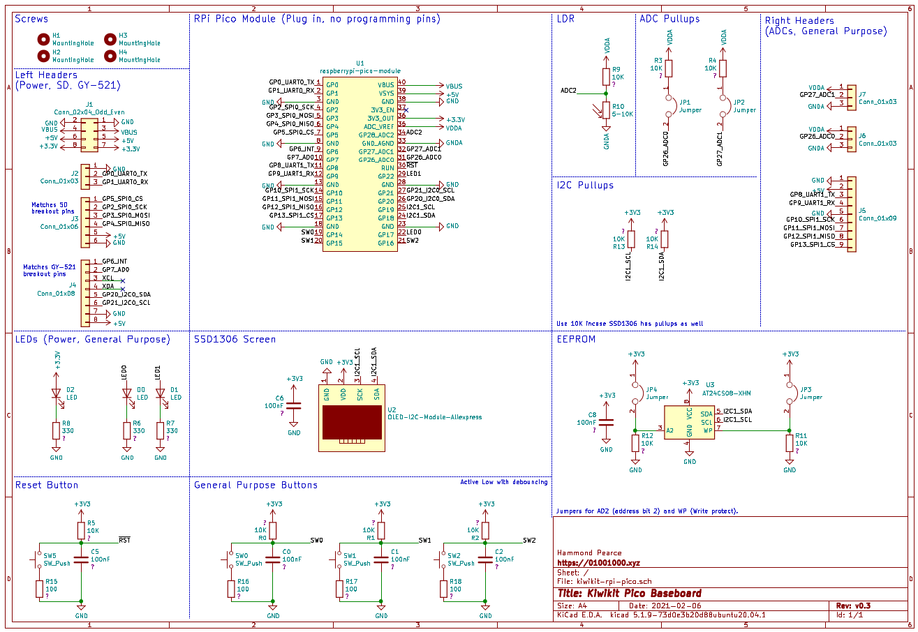
You can see that doing layouts like this also really shows off how simple everything is. Here’s a couple of quick design decisions:
- I used a standard layout for switch debouncing. These values are all pretty flexible.
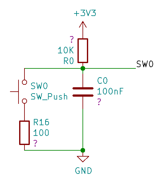
Note that the question marks (?) are present because the parts are missing Vendor codes - this is because they’re going to be supplied from my parts bin :)
- I have 10K pullups on the I2C line.
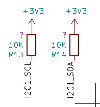
I used these since the SSD1306 modules have inconsistent pull-ups - sometimes they are fitted, sometimes they aren’t (such is the way of aliexpress). If we use 10K, additional pull-ups (which will probably also be 10K) won’t bring the pull-up resistance too low. An alternative would have been to jumper these (I’ve done that in the past), but on previous dev boards I found I was never removing the jumpers.
- 5K pullups on the LDR and other two ADCs (with jumpers to make them optional). The LDRs I have range from 5-10K, so 5K gives a reasonable range in sensed voltages when constructed as a voltage divider.
- Jumpers on the EEPROM - WP (Write protect) and A2 (Second bit of I2C address).
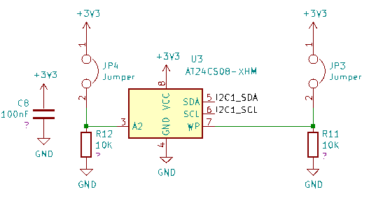
It’s tenuous, but if a different screen was in use in future that conflicted with the EEPROM address, the A2 jumper could be used to move the EEPROM slightly. The WP pin gives us the ability to disable writes to the EEPROM, should such a situation ever be useful.
In the layout
This is a pretty subjective area and design choices can be a little harder to justify. Technologically, I went for a 2 layer board (cheap), and 10cm x 10cm (since that gave me more space for the larger through-hole components). Since I was going with JLCPCB for production, I made sure that the board fit their design requirements. I actually went far too conservative, setting my minimum track width to 0.3mm and via hole size to 0.4mm.
Anyway, any developer will tell you that the most important thing is to make sure your corners are rounded since PCBs can be sharp,
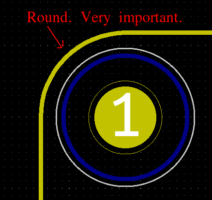
(It also helps to add screwholes for mounting!)
I made a custom footprint for the Pico module based on the Pico’s datasheet, Chapter 2. Since I want to keep in the spirit of breadboarding, I assume that the debugging pins on the modules are either not soldered or are soldered “up”, so I didn’t include them in the footprint (for the same reason, they also weren’t included in the schematic). The footprint, embedded in the circuit, is depicted here:
I went for an assymetric look, with the Pico off to the top-left, and the SSD1306 down at the bottom-right. The AT24 is neatly placed above the SSD1306. Assuming that the buttons would be used in tandem with the screen, the three general purpose buttons are placed directly beneath, with their debouncing resistors and caps placed in neat lines off to the side. The reset button is in the top right (someone called me out on this, but I like my reset buttons to be distinct from other buttons - they have quite different purposes!). The LDR is placed in the middle of the top of the board, and the power LED is on the far left. Other support components are arranged neatly into lines, and finally the breakout pins are organised down each side of the board.
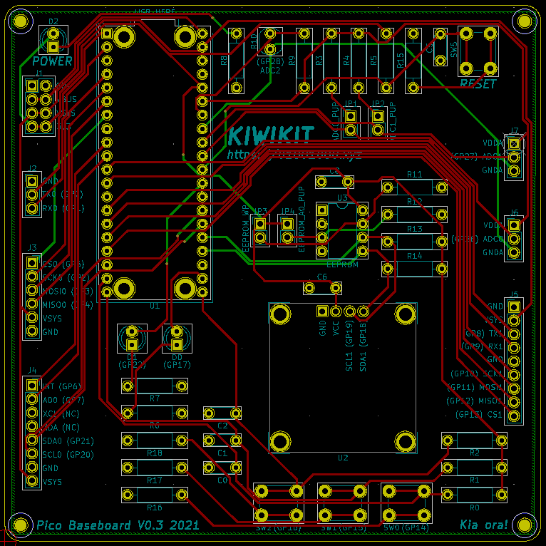
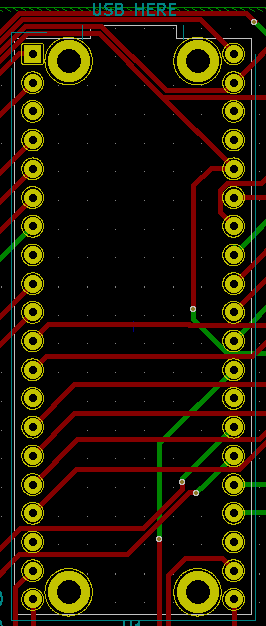
Overall routing was a breeze. Almost every trace could be kept on the top of the board, leaving the bottom layer as an almost completely unbroken ground plane, which is great for signal integrity.
A top tip: when you find yourself routing a microcontroller (or a microcontroller module), remember that peripheral pins often have more than one option for their location! As such, you can often move where things are assigned to simplify the routing process / untangle any messes. E.g., from the manual linked above (Figure Copyright 2020 Raspberry Pi (Trading) Ltd.CC-BY-ND).
We used I2C1 for the SSD1306/EEPROM - look how many different places we could have routed that!
3D modelling
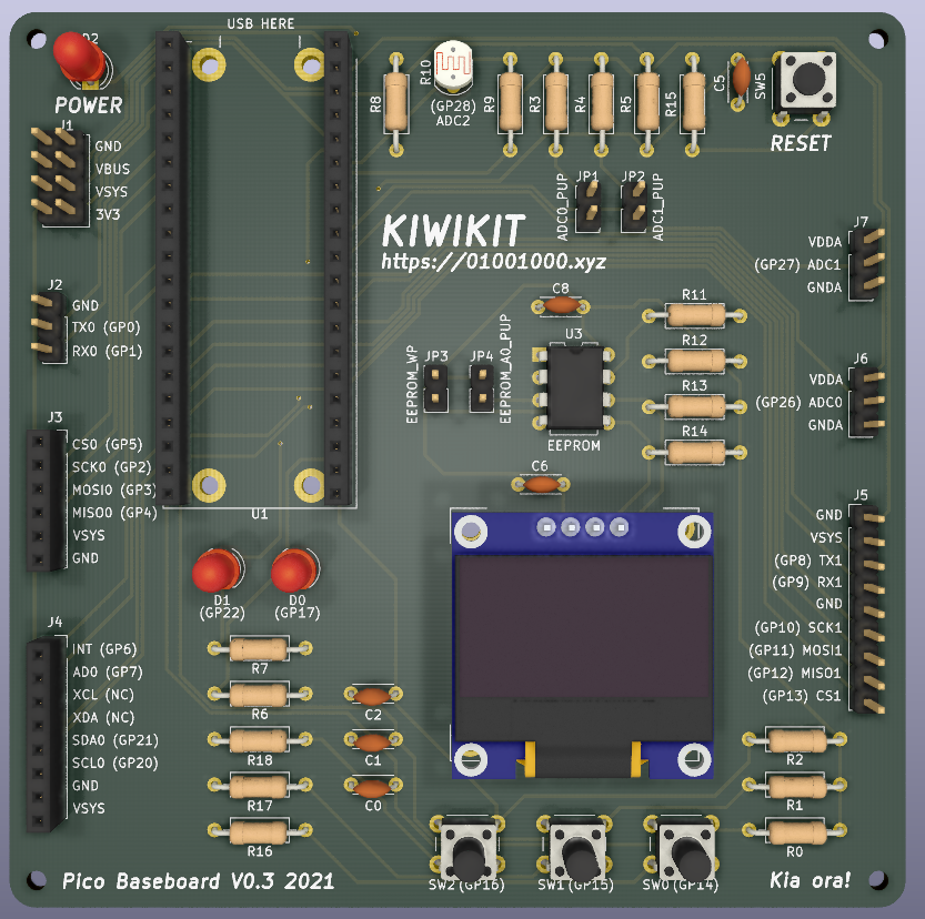
I always like to make sure I have 3D models of all the components so that I can visualize how it will all fit together. It’s a nice sanity check. Kicad makes this easy, and the 3D model viewer can read in 3D models for your components and place them where they should be.
Getting it manufactured
I’ve used a few of the different online manufacturers, but the one I usually go back to is JLCPCB, so that’s who I went with this time (Note, not an advert). Their quality is pretty good, and they have nice guides for Kicad which I appreciate.
Following the steps, I produced and uploaded a gerber zip, paid the $2 for manufacture (for 10! wow!) and the $15 for shipping (sad US-China trade war / covid noises), and 2 weeks later they arrived!
NOTE: Photos in this section are of the V0.1 board compared with the V0.3 designs above. The changes were cosmetic (silk screen), and I added an extra resistor to each debouncer.
![]()
Now I had to solder them up:
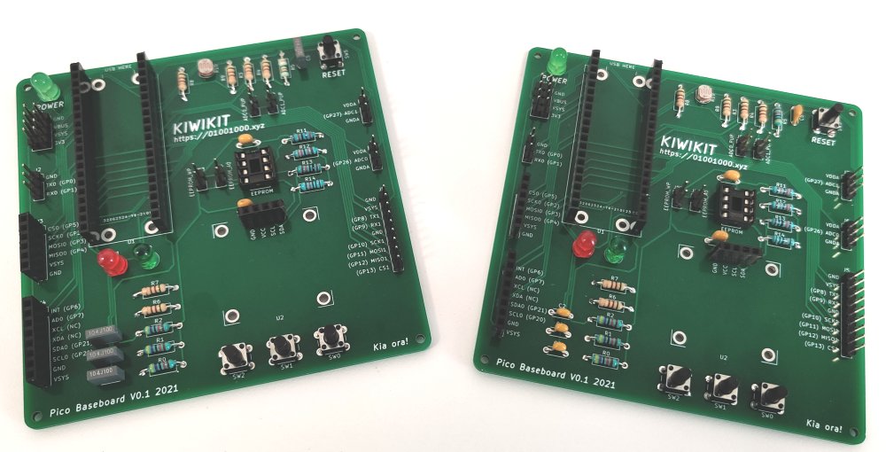
And test them!
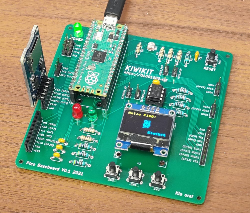
And that’s that! I wrote up a quick MicroPython script to test everything out, and got a resounding pass in every category - well, except for the lower green general purpose LED, which is really dim for some reason (thanks component bin / quality testing before soldering things on).
Anyway, I’m pretty happy with it!
The design files
If you want to manufacture this board yourself, feel free! On my Github I have released these files under the open MIT license, and I encourage usage / modification / pull requests. Enjoy (if you want)!